Work / Fig 02 · 2026–
Homemade semiconductor
A lab-in-progress: homemade microchips via maskless stereolithography on a 4" P-type wafer, targeting ~100 μm features with off-the-shelf hardware. Calibration pattern is printing. Devices are not.
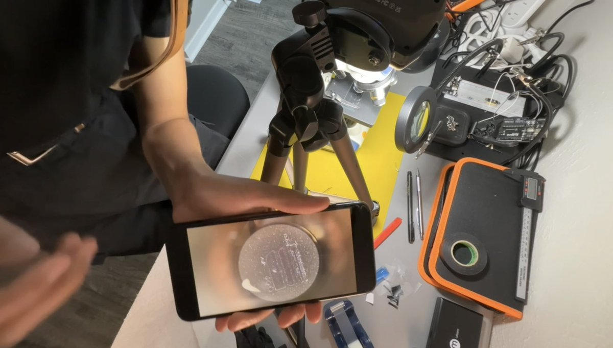
A bench lab for homemade chips: a 4" wafer in a carrier ring rides a 4K mSLA printer's Z tower down onto its UV LCD, the screen lights a calibration pattern of 100 μm and 250 μm lines for an exposure, and the wafer lifts away; a stereo microscope and a wafer case sit beside it.
Maskless mSLA · ~100 μm calibration · in progress
Status
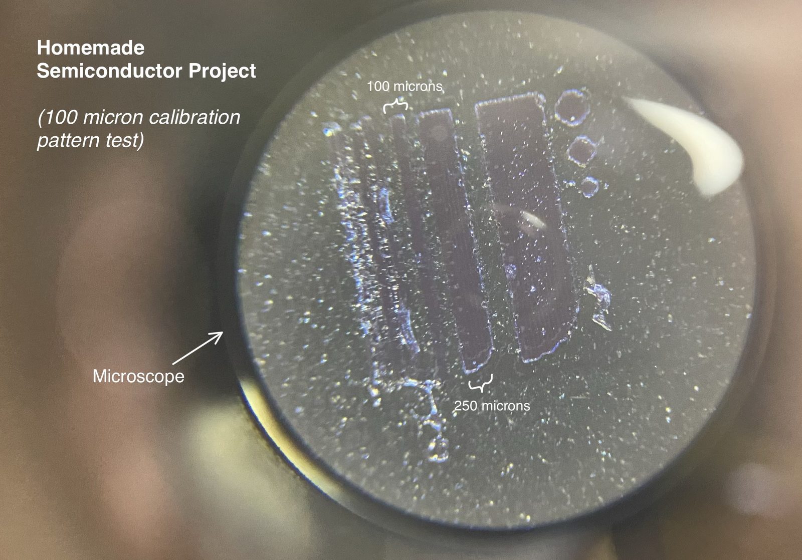
In progress. The public artifacts so far are a 4" wafer, a maskless mSLA exposure path, and a calibration pattern that is resolving at about 100–105 μm.
This is not a foundry, not a product, and not a finished die. It is a notebook with photographs.
The stack that is actually on the bench
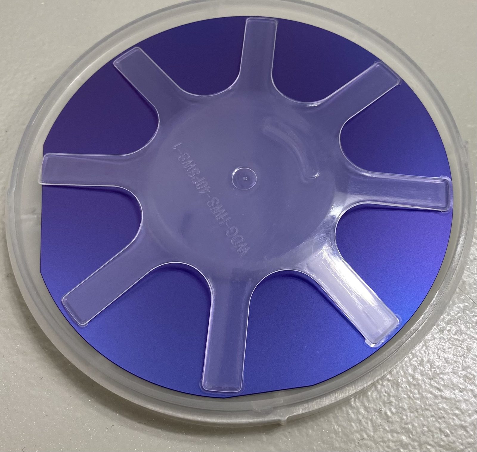
4" P-type boron-doped wafer, 500±25 μm thick, with a 300 nm thermally grown silicon dioxide layer. Exposure through a 4K maskless stereolithography printer (~35×35 μm pixel). Ultrasonic sodium carbonate bath for uniform agitation and developed photoresist removal. Exposure time, development time, and agitation are what is being tuned.
The calibration target is a line-width pattern at 100 μm and 250 μm. That is the photograph. Feature size is still two orders of magnitude above the 50–1000 nm thesis — this lab is building process intuition, not claiming a node.
Why it exists
The dispatch argues for dirt-cheap 50–1000 nm silicon on American soil: sub-PCB integration without EUV cathedrals. This lab is the hands-on half of that argument. Maskless UV at coarse features is how a single engineer even starts.
The diagram on the flag is the thesis geometry. The microscope photograph is the current evidence.
Stack
Links
Interactive figure · Maskless Lithography Bench
Open on its own ↗The bench in one figure: the LCD as a programmable mask, the bath, the microscope. Pick a pattern, set the dose, run a cycle.
From the bench
3 images